
- English
- Español
- Português
- русский
- Français
- 日本語
- Deutsch
- tiếng Việt
- Italiano
- Nederlands
- ภาษาไทย
- Polski
- 한국어
- Svenska
- magyar
- Malay
- বাংলা ভাষার
- Dansk
- Suomi
- हिन्दी
- Pilipino
- Türkçe
- Gaeilge
- العربية
- Indonesia
- Norsk
- تمل
- český
- ελληνικά
- український
- Javanese
- فارسی
- தமிழ்
- తెలుగు
- नेपाली
- Burmese
- български
- ລາວ
- Latine
- Қазақша
- Euskal
- Azərbaycan
- Slovenský jazyk
- Македонски
- Lietuvos
- Eesti Keel
- Română
- Slovenski
- मराठी
- Srpski језик


Cina CVD SIC Produttori, Fornitori, Fabbrica
CVD SiC is a vacuum deposition process used to produce high-purity solid materials. This process is often used in semiconductor manufacturing to form thin films on wafer surfaces. During the chemical vapor deposition (CVD) process for producing silicon carbide (SiC), a substrate is exposed to one or more volatile precursors, which chemically react on the substrate surface to form the desired SiC deposit. Among the various methods for producing SiC, CVD produces products with high uniformity and purity, and offers strong process controllability.
Simply put, CVD SiC refers to SiC produced via the chemical vapor deposition (CVD) process. In this process, gaseous precursors, typically containing silicon and carbon, react in a high-temperature reactor to deposit a thin SiC film onto a substrate. CVD SiC is valued for its exceptional properties, including high thermal conductivity, chemical inertness, mechanical strength, and resistance to thermal shock and wear. These properties make chemical vapor deposited (CVD) silicon carbide (SiC) ideal for demanding applications such as semiconductor manufacturing, aerospace components, armor, and high-performance coatings. This material's exceptional durability and stability under extreme conditions ensure its effectiveness in improving the performance and lifespan of advanced technologies and industrial systems.
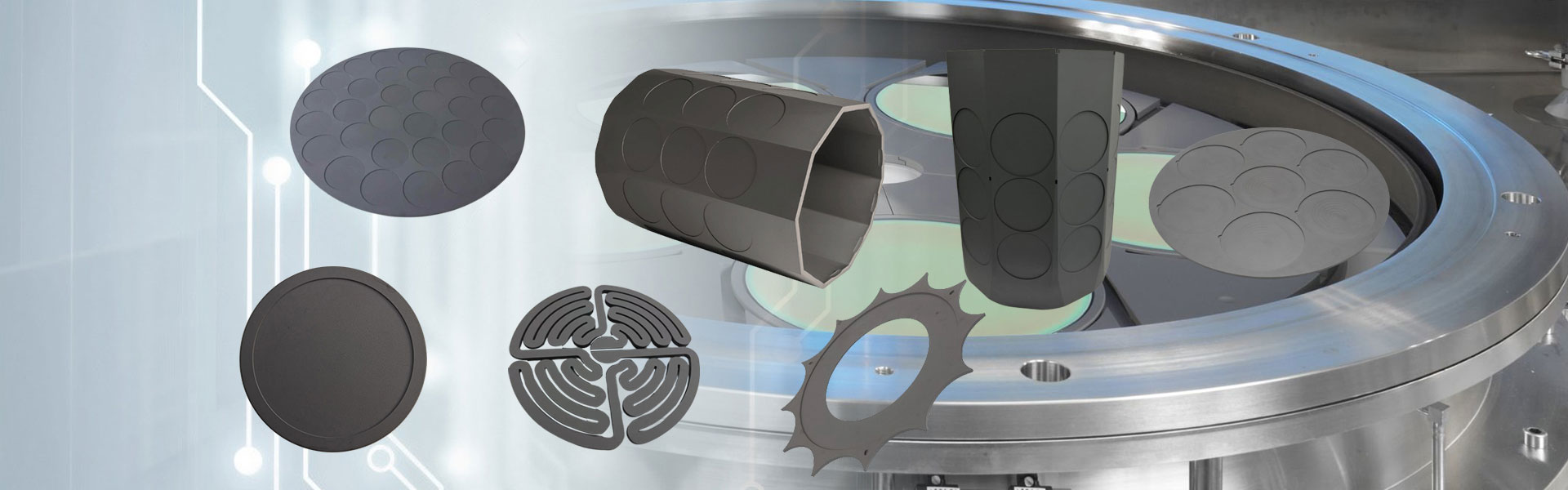
CVD SiC materials, due to their unique combination of excellent thermal, electrical, and chemical properties, are well-suited for applications in the semiconductor industry, where high-performance materials are required. Chemical vapor deposited (CVD) silicon carbide (SiC) components are widely used in etching equipment, MOCVD equipment, Si and SiC epitaxy equipment, and rapid thermal processing equipment.
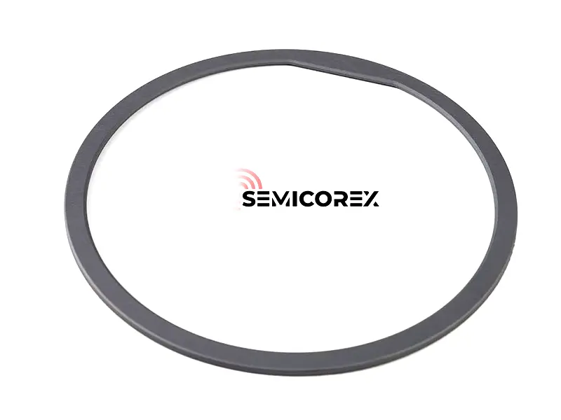
The largest market segment for CVD SiC components is etching equipment components. Due to its low reactivity to chlorine- and fluorine-containing etching gases and its electrical conductivity, CVD silicon carbide (SiC) is an ideal material for components such as focus rings in plasma etching equipment. CVD silicon carbide (SiC) components in etching equipment include focus rings, gas showerheads, trays, edge rings.
Take the focus ring, for example. This critical component is placed outside the wafer and in direct contact with it. Voltage is applied to the ring to focus the plasma passing through it, thereby focusing the plasma on the wafer and improving processing uniformity. Traditionally, focus rings are made of silicon or quartz. However, with the advancement of integrated circuit miniaturization, the demand for and importance of etching processes in integrated circuit manufacturing continues to increase. The power and energy of the plasma used for etching are also increasing, especially in capacitively coupled plasma (CCP) etching equipment, which requires even higher plasma energies. Consequently, focus rings made of silicon carbide are becoming increasingly popular.
Due to the high performance of CVD SiC and its ability to be sliced into very thin sections, it can also benefit sputter targets and all types of electrodes.
Process of Chemical Vapor Deposition (CVD)
CVD is a process that transforms a material from a gas phase to a solid phase, used to form a thin film or coating on a substrate surface. The following are the basic steps in CVD:
1. Substrate Preparation
Choose an appropriate substrate material and perform the appropriate cleaning and surface treating to produce a clean, flat surface with good adhesion.
2. Reactive Gas Preparation
Prepare the necessary amount of reactive gas or vapor and inject it into the deposition chamber by some means (gas supply system). The reactive gas can be an organic compound, a metal-organic precursor, inert gas, or other gaseous species.
3. Deposition Reaction
If all instrumentation is setup correctly the CVD process will begin under the pre-defined reaction conditions. The reactive gas that has been injected into the chamber will undergo some chemical or physical reaction on the substrate surface to form a deposit onto the substrate surface. The deposit formation can be the result of several types of processes depending on the deposition method, these include vapor-phase thermal decomposition, chemical reaction, sputtering, epitaxial growth, etc.
4. Control and Monitoring
At the same time during the deposition process, certain deposition parameters need to be controlled and monitored in real time if the observer wishes to ensure the best possible properties in the film are maintained. These include relevant temperature measurement, pressure monitoring, and regulation of gas flow, all the while aiming to keep the desired reaction conditions stable and constant.
5. Deposition Completion and Post-Processing
When either the deposition time, predetermined thickness, or method selected, is achieved the introduction of the reaction gas can be ceased and deposition process ended. Following the deposition, several pertinent post-processing methods (annealing, structural modifications, surface treatment, etc.) should be performed to improve the film performance/quality.
It's important to note that the specific vapor deposition process can vary depending on the deposition technology, material type, and application requirements. However, the basic process outlined above covers most common vapor deposition steps.
- View as

Soffioni doccia CVD SiC
I soffioni doccia Semicorex CVD SiC sono componenti di elevata purezza e ingegneria di precisione progettati per sistemi di incisione CCP e ICP nella produzione avanzata di semiconduttori. Scegliere Semicorex significa ottenere soluzioni affidabili con purezza del materiale, precisione di lavorazione e durata superiori per i processi al plasma più impegnativi.*
Per saperne di piùInvia richiesta
Anelli per bordi
Gli anelli di semirex bordo sono affidabili dai principali FAB e OEM di semiconduttore in tutto il mondo. Con un controllo di qualità rigoroso, processi di produzione avanzati e progettazione basata sull'applicazione, Semicorex fornisce soluzioni che prolungano la durata dello strumento, ottimizzano l'uniformità del wafer e supportano i nodi di processo avanzati.*
Per saperne di piùInvia richiesta
Piastre di distribuzione del gas
Le piastre di distribuzione di gas Semicorex, realizzate in CVD SIC sono un componente critico nei sistemi di incisione al plasma, progettate per garantire una dispersione di gas uniforme e prestazioni al plasma coerenti attraverso il wafer. Semicorex è la scelta affidabile per soluzioni in ceramica ad alte prestazioni, offrendo purezza di materiale senza pari, precisione ingegneristica e supporto affidabile su misura per le esigenze della produzione avanzata di semiconduttori.*
Per saperne di piùInvia richiesta
Soffione doccia in SiC solido
Il soffione doccia Solid SiC è un componente cruciale nella produzione di semiconduttori, progettato specificamente per i processi di deposizione chimica da fase vapore (CVD). Semicorex, leader nella tecnologia dei materiali avanzati, offre soffioni doccia Solid SiC che garantiscono una distribuzione superiore dei gas precursori sulle superfici del substrato. Questa precisione è vitale per ottenere risultati di elaborazione uniformi e di alta qualità.**
Per saperne di piùInvia richiesta
Anello di messa a fuoco CVD SiC
Attraverso un processo di deposizione chimica da fase vapore (CVD), l'anello di messa a fuoco SiC Semicorex CVD viene meticolosamente depositato e lavorato meccanicamente per ottenere il prodotto finale. Grazie alle proprietà superiori del materiale, è indispensabile negli ambienti esigenti della moderna fabbricazione di semiconduttori.**
Per saperne di piùInvia richiesta
Anello di acquaforte
L'anello di incisione in CVD SiC è un componente essenziale nel processo di produzione dei semiconduttori, offrendo prestazioni eccezionali negli ambienti di incisione al plasma. Grazie alla sua durezza superiore, resistenza chimica, stabilità termica ed elevata purezza, CVD SiC garantisce che il processo di incisione sia preciso, efficiente e affidabile. Scegliendo gli anelli di incisione SiC CVD Semicorex, i produttori di semiconduttori possono aumentare la longevità delle loro apparecchiature, ridurre i tempi di inattività e migliorare la qualità complessiva dei loro prodotti.*
Per saperne di piùInvia richiesta
Semicorex produce CVD SIC da molti anni ed è uno dei produttori e fornitori CVD SIC professionali in Cina. Una volta acquistati i nostri prodotti avanzati e durevoli che forniscono imballaggi sfusi, garantiamo la grande quantità in consegna rapida. Nel corso degli anni, abbiamo fornito ai clienti un servizio personalizzato. I clienti sono soddisfatti dei nostri prodotti e del servizio eccellente. Non vediamo l'ora di diventare il vostro partner commerciale affidabile a lungo termine! Benvenuti a comprare prodotti dalla nostra fabbrica.